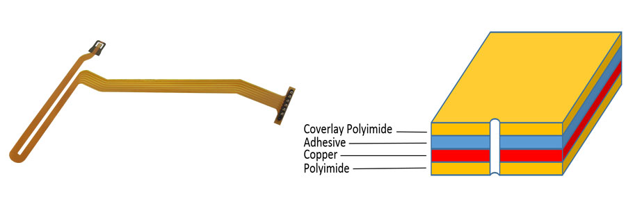
Single Side FPC
- Consists of a single conductor layer of metal or conductive polymer on a flexible dielectric film.
- Component termination features are accessible only from one side, with holes in the base film for component assembly.

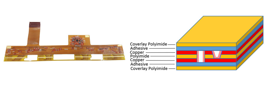
Double Side FPC
- Consists of 2 conductive layers fabricated with or without plated through holes.
- When constructed without plated through hole, the connection features are accessible only from one side.
- Because of the plated through hole, terminators for electronics components are provided on both sides of the circuit, allowing components to be placed on either side.

Multi Layered Flex Circuit
- Consists of 3 or more layers of conductive and are also known as multilayer flex circuit.
- Layers are interconnected by plated through hole or openings to access lower circuit level features.
- Discontinuous lamination is common in cases that require maximum flexibility or bending.

Bare Backed Flex Circuit
- Bare Back Flex Circuit (double access) has a single conductor layer that allows access to features of the conductor pattern such as lead termination from both sides.
- This is not commonly manufactured because of the special processing required to provide access to the features discretely.

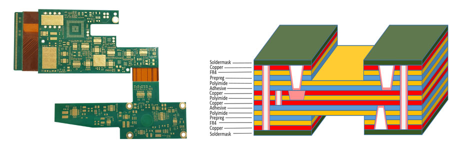
Rigid Flex Circuit
- Hybrid constructions consists of flexible and rigid substrates are laminated together into a single structure and then electrically interconnected using plated through hole.

Rigid Flex Features
- No. of layer count from 1 to 12 layers.
- Board thickness from 0.20mm to 2.4mm.
- Blind/Buried via plating.
- Impedance control
- Static/multiple bending
Special Process
- Control depth drilling & routing
- Blind via filled plating
- Edge platiing
Application
- Automotive
- Medical
- Industrial
- Telecom
FPC Features
- Flexible, space‐saving, resolves mechanical constraints, supports dynamic applications.
- Provides one‐stop assembly service.
- Full range of products: Single‐Sided, Double‐Sided, Bare Backed & Multi‐Layer board.
- Split foil (air gap) un‐bond area for increasing flexibility.
- Flying leads.
- Impedance control.
- Fine pitch SMD / BGAs.
- Multiple finishing.
- ZIF finger control ±0.05mm.
- Bonded with stiffeners, including metal, PI, FR4, PET material.
- Laminated with EMI shielding, include silver foil, copper foil,silver paste printing.
Special Process
- Laser skiving on PI
- Encapsulation
- Blind via filled plating
- Dimple formation
Application
- Data Storage
- Medical
- Automotive
- Industrial
- Consumer
- Tele-communication
- Display Modules
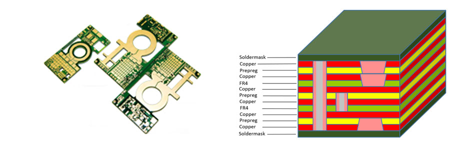
Rigid PCB
Rigid PCB circuit consists of conducting layers made of copper foil and insulating layers dielectric that are typically laminated together with epoxy resin prepreg. The board is typically coated with solder mask.

PCB Features
Suitable for BGA with smaller ball pitch and higher I/O counts
- Thin board capabilities down to 0.25mm
- Increase routing density in complicated design
- Silver / copper plated through hole, via in pad
- Lower Dk / Df material enables better signal transmission performance
- Buried, blind & stack vias
- Heavy copper weight
- Impedance control
Special Process
- Control depth drilling & routing
- Embedded copper coin
- Beveling gold finger
- Copper plating on top of resin plugging via
- Plating edge
Application
- Automotive
- Power Supply
- Industrial
- Energy
- Planar Transformer e.g. ER11T216321
- Board Mounted Power (BMP)
- 4G LTE Base Station
- LCD Modules

